
Have you ever wandered the streets wondering, ‘Boy o boy! I wish I had more control over my life!’? Well! Wander no more and come into my parlour as I take you through the exciting world of power control. In this article, you’ll learn to take control of your life by designing a simple PWM control circuit that drives a MOSFET. Underlying this little circuit is a 555 timer. Adjust the frequency using the capacitors, add a variable resistor – and voila! Power control! I designed this controller for use with a simple hot wire foam cutter.
I’ve created a schematic for this controller using a simple, yet wonderful, little software called LTSpice. The neat thing about LTSpice is that you can actually simulate your circuit (via SPICE) to see whether it works. You can see this schematic below in figure 1. Essentially this circuit produces a high power pulse width modulated (PWM) output at a specific frequency. There are tons and tons of things to explain – so let’s get started!
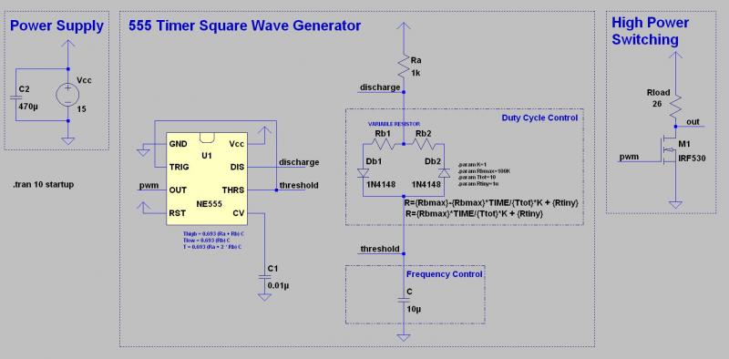
Power Supply
The circuit uses a normal wall or laptop DC power supply. In the circuit this is represented by Vcc. This value is set to 15 V and is used both to drive the low power circuitry of the 555 timer and the high power circuit of the MOSFET switch. The NE555 timer’s absolute maximum supply voltage is not particularly high (18 V), so increasing this Vcc a great deal more is likely to damage the circuit.
There are cases when you absolutely positively need a higher voltage at the MOSFET. If that’s the case, we can regulate the voltage down for the 555 timer and its associated circuitry. Be warned, the gate voltage must be high enough and the current supplied by the timer high enough to drive the MOSFET into saturation (fully on). For the IRF530 the gate-source voltage Vgs needs to be around 10 V for this to happen.
The power supply should also be capacitively filtered to remove high frequency noise. How essential this is, depends on the wall adapter that you’re using. Adapters for laptops typically provide lower noise power output and may not need to be filtered.
R = {R_{\:bmax}} \cdot K \cdot \frac{TIME}{T_{\:tot}} + {R_{\:tiny}}The 555 timer provides us with highly configurable square wave function generator features. The circuit shown in figure 1 operates in astable mode. Figure 2 shows the biasing of the timer circuit in astable mode. We can find a detailed explanation of how a 555 timer works in the NE555 datasheet.
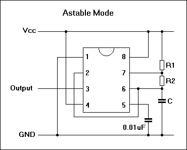
Looking at this circuit we can describe the output square wave with the following formulation:
\begin{aligned}
T_{\:high} &= 0.693 \cdot (R_{\:1} + 2 \cdot R_{\:2}) \cdot C \\ \; \\
T_{\:low} &= 0.693 \cdot R_{\:1} \cdot C \\ \; \\
T &= T_{\:low} + T_{\:high} \\ \; \\
f = \frac{1}{T} &= \frac{1.44}{ (R_{\:1} + 2 \cdot R_{\:2}) \cdot C }
\end{aligned}
This circuit is taken from an NE555 datasheet. In the case of our oscillator circuit, R1 = Ra and R2 = Rb. In addition to a resistor, we also have two 1N4148 diodes connected to our resistor Rb. But wait. Where is Rb in figure 1???
Variable Resistors in LTSpice
The two resistors, Rb1 and Rb2, in figure 1, actually form our one Rb resistor. Rb is a variable resistor. Currently there’s no convenient way to change the resistance dynamically in an LTSpice simulation. So, for simulation purposes, I’ve separated Rb into two resistors whose resistance changes over time. This is done by defining the values of each of the resistors such that:
For Rb1
R = {R_{\:bmax}} - {R_{\:bmax}} \cdot K \cdot \frac{TIME}{T_{\:tot}} + {R_{\:tiny}}For Rb2
R = {R_{\:bmax}} \cdot K \cdot \frac{TIME}{T_{\:tot}} + {R_{\:tiny}}Rb is actually a 100KΩ variable resistor. The above two formulae are input as values for Rb1 and Rb2 via LTSpice. This sweeps through all values of the resistor, Rb, for the time period over which the simulation is running. Rbmax is the actual value of Rb, 100KΩ. I used a total running time for the simulation Ttot = 10 s. The variable, TIME is the current simulation time. If resistance ever reaches a zero value the results of some computations can become undefined. To prevent this from happening, I’ve added an extra tiny resistance, Rtiny = 1 μΩ for simulation purposes. Lastly, the value K is a boolean used so that the variable resistor behaviour of Rb can be disabled, if needed.
Trigger, Threshold and Discharge
Pin 2 is the trigger and acts as a start signal to get the timer running. The trigger is active low and so starts the timer when the voltage on the drops below one-third of the supply voltage, Vcc. When the trigger value goes low, the output on pin 3 goes high. The trigger pin monitors the voltage at capacitor C.
Pin 7 is called the discharge. This pin is used to discharge an external capacitor, C. This capacitor combined with Ra and Rb control the timing of the waveform. During discharge the discharge pin sinks current through C and Rb2. Thus the combination of these two components determines how long it takes for the trigger input to reach a low value and hence a high output.
Pin6 is called the threshold. The pin monitors the voltage on the capacitor, C. When this voltage rises above two-thirds of Vcc the threshold pin causes the output on pin3 to go low. The capacitor, C, is charged through resistors Ra and Rb1 in figure 1. So the combination of these three components controls how long it takes for the threshold input to reach a high value and hence a low output.
Changing the values of Ra, Rb, C will also change the frequency of our wave form. We use opposite ends of the variable resistor Rb, with the centre lead connected to Ra for this reason – we don’t want a resultant frequency change when we vary the resistance. We can however control the frequency by change the capacitor, C or Ra. Now the problem with changing Ra is that it also has some effect on the duty cycle – ideally it should be kept as small as possible. As we’ll see in figure 2, this resistor is the reason we can’t quite reach a full 100% duty cycle or full 0% duty cycle. Instead our duty cycle varies from around 10% to around 90%. One question that might pop into your head, then, is: “Why use Ra at all?”. Well, I’m not really sure. But I’ll hazard a guess. Since the discharge pin sinks current, you want to make sure that there is a limit to the amount of current – the discharge pin is the collector end of an internal NPN transistor and the transistor needs to be properly biased.
High Power Switch
I’m using an IRF530 n-channel MOSFET to act as my high current switch. This MOSFET can be replaced by any range of other MOSFETs, as long as the current in the resistive load Rload doesn’t exceed the specs. Another MOSFET worth considering is the IRFZ44. This MOSFET has a much lower resistance between its drain and source meaning that it will remain cooler during operation and thus can tolerate much higher currents of upto 60 A absolute maximum. The IRF530 can only manage around 14 A absolute maximum.
Simulations
So what happens when we actually try to simulate this circuit? Well, the figure below shows the output of the circuit MOSFET when connected to a 26 Ω resistive load. Notice that the duty cycle in the below circuit varies over time – that’s because the variable resistor Rb is setup to go over its entire range from 0 Ω to 100 KΩ over the runtime of the simulation.
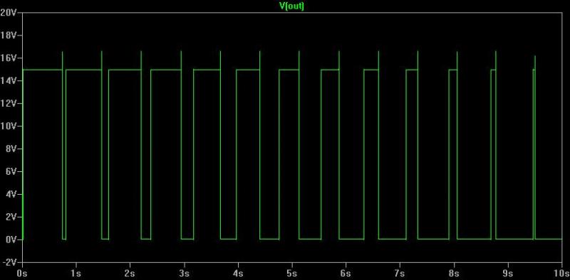
Notice that there are some voltage spikes at the output. The actual PWM signal input into the high power switch does not contain the spikes. I don’t really know why these high frequency spikes are there.
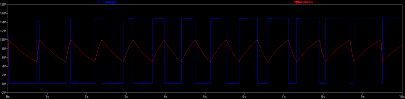
The next figure (figure 3) shows what happens at the threshold and trigger pins during the course of the simulation. Again, the lengthening of the waveform is a result of the variable resistor’s value changing over the course of the simulation. In reality, this resistor would be fixed at a specific value and so no changes would occur over time and the duty cycle would remain constant.
Hot Wire Cutter
Now that we have gone over a circuit. We can start looking at designing a mechanical structure for a Hot Wire Cutter based on this circuit. I started this by doing a CAD design as shown with the draft below with the aim of 3D printing it.
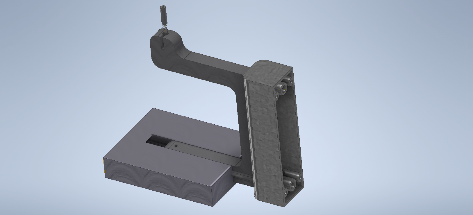
But realized that it was more work than it was worth so abandoned the design mid way through in favour of just use bits and pieces lying around the house to put something together really quickly. The pictures below are the result of this hack job.
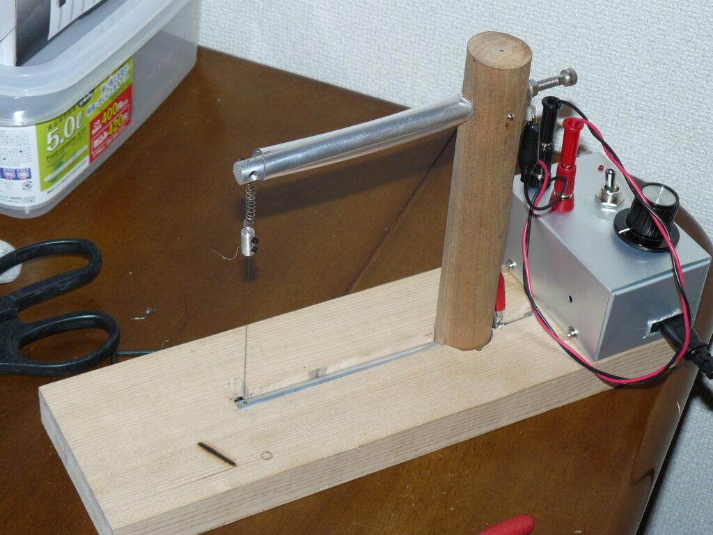
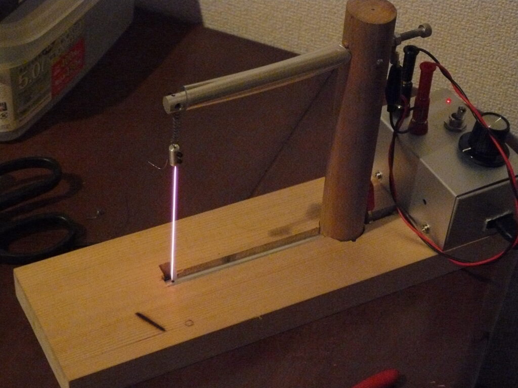
The knob controls the power to the nichrome wire. Moving up the power level to about the half way mark shows that you can really get the wire hot to a level that can cut through harder plastics. Though doing this myself I found that the plastic would cool around the cut and melt together behind the hot wire making it hard to remove the wire.
The spring is there to tension the hot wire as it heats up so that it stays taught for more accurate cutting. But putting the wire under too much tension can easily cause it break especially during heating at high temperatures. Aluminium rods are used to conduct the current to the hot wire. I’ve drilled a hole through the rod and threaded it to fit a set screw. The set screw then holds the spring. I used a smaller Aluminium rod cut to size with a center hole and two threaded holes with set screws to secure the hot wire to the spring. I’ve also threaded the back of the aluminium rods to allow attachment of wires – in the end I just used aligator clips.
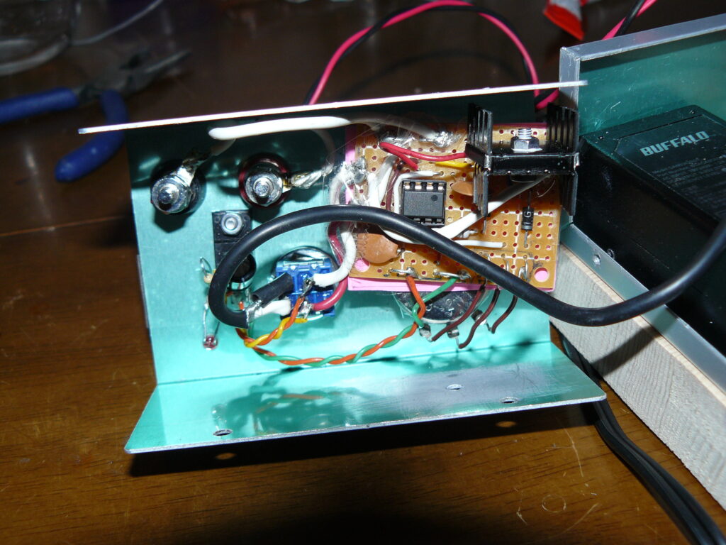
Below is my ‘quick as possible’ hack job of putting the 555 timer on a proto-board and into a project box with knob and plugs.
Downloads
If you want to play around with the files for this project, you can download them below. Basically, inside you can find some LTSpice files as well as the waveforms and some design notes.